



Processing Challenges of Key Components of Third-Generation Semiconductors
As core components of third-generation semiconductors, silicon carbide wafer trays and chucks are widely used in high-temperature and high-frequency devices due to their corrosion resistance and high thermal conductivity. However, silicon carbide has a hardness of up to HV2,002, and problems such as chipping, substandard flatness and finish are prone to occur during processing. Traditional processes are inefficient and costly, which has become a pain point restricting the development of the industry.
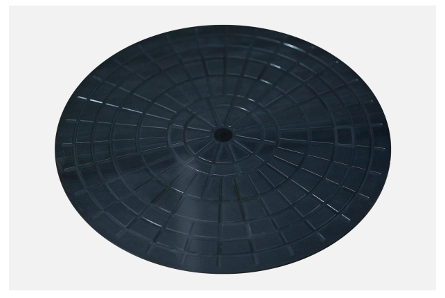
Case Focus: Silicon Carbide Wafer Tray Chuck Processing
Processing Product Parameters
Material: Silicon Carbide (SiC)
Features: Precision Grinding of Cavity and Groove Structure
Size: Diameter 380mm × Thickness 5mm
Hardness: HV2,002 (close to the hardness of natural diamond)
Background and Difficulty Analysis
1.Industry Demand : With the trend of miniaturization and high performance of semiconductor equipment, silicon carbide components need to have both complex structures and ultra-high precision.
2.Processing Difficulties :
High chipping risk: The material is brittle, and improper cutting force control can easily lead to edge defects.
Fast tool wear: The life of traditional tools is less than 159 minutes, and frequent tool changes affect production capacity.
Low efficiency: Single-piece processing takes up to 888 minutes, which is difficult to meet mass production needs.
MID solutions: Ultrasonic precision machining technology subverts traditional processes
Aiming at the pain points of silicon carbide processing, MID solutions proposes an innovative technology combination:
Ultrasonic precision engraving and milling: Reduce cutting resistance and material stress concentration through high-frequency vibration, and suppress chipping from the source.
Integral PCD micro-blade milling cutter: Adopt polycrystalline diamond (PCD) superhard tools, with blade accuracy of micron level, taking into account wear resistance and cutting stability.
Intelligent optimization of process parameters: Match ultrasonic amplitude and feed speed to achieve a balance between material removal rate and surface quality.
Double breakthrough in efficiency and cost
After applying MID solutions, the processing of silicon carbide parts has been significantly improved:
The chipping rate has dropped by 60%: Ultrasonic technology reduces cutting force by 45%, and the edge integrity reaches the Ra0.2μm finish standard.
Efficiency increased by 48%: Single-piece processing time was reduced from 888 minutes to 462 minutes, and production capacity doubled.
Tool life doubled: PCD tool working time was extended from 159 minutes to 317 minutes, and direct costs were reduced by 35%.
About MID
MID (Mid Technology) has been focusing on precision machining for more than ten years and is committed to providing high-difficulty material processing solutions for semiconductor, optics, aerospace and other industries. The company takes ultrasonic assisted machining technology as the core, combined with self-developed tools and intelligent process systems, to help customers break through efficiency bottlenecks and achieve domestic substitution of high-end manufacturing.


