



In the field of precision manufacturing, single crystal silicon is known as the "cornerstone of the information age" - from smartphone chips to optical components of space satellites, from new energy photovoltaic cells to core devices of quantum computing, this high-purity, near-perfect crystal material has always played the underlying supporting role of disruptive technology. As semiconductor technology enters the process below 3 nanometers and photovoltaic cell efficiency breaks through the theoretical limit, the market's requirements for single crystal silicon processing accuracy have jumped from micron level to nanometer level. Especially in the processing of complex structures such as curved electrode drilling, the contradiction between the high brittleness of the material, the crystal directional cleavage characteristics and the nanometer-level aperture tolerance is becoming a key bottleneck restricting the development of cutting-edge industries such as high-end chip manufacturing and high-energy particle detectors.
Industry Breakthrough Record
Ultra-deep micro-hole processing of single crystal silicon: from "stuck neck" to "Chinese solution"
Case background
When a leading domestic semiconductor equipment company was developing core components of 3D NAND storage chips, it encountered the extreme challenge of ultra-deep micro-hole processing of single crystal silicon: it was necessary to process micro-holes with a diameter of only 0.45mm on a silicon substrate with a thickness of 24.75mm (depth-to-diameter ratio of 55:1), and its precision requirements were comparable to "carving a kilometer-deep well on a hair". Previously, this type of process had long been monopolized by Japanese and German companies. Domestic manufacturers not only had to pay an import cost of more than 10,000 yuan per piece, but also faced supply chain risks caused by technological blockades.
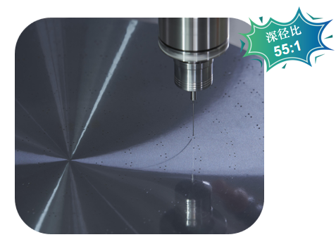
Pain point direct attack
Precision out of control: After processing with traditional carbide drills, the hole wall roughness Sa≥6.54μm (3 times the industry standard), and the roundness deviation>0.025mm, directly leading to a surge in chip signal transmission loss rate;
Yield curse: The cost of monocrystalline silicon raw materials accounts for more than 60%, but defects such as edge collapse and microcracks cause the workpiece scrap rate to be as high as 35%, and the company's annual loss exceeds 20 million yuan;
Technology gap: Overseas equipment prohibits Chinese manufacturers from using core algorithm modules such as "dynamic vibration suppression", and there is no mature domestic process to replace it.
MID Solution
MID precision machining successfully solved the above problems through ultrasonic auxiliary system + nanocrystalline PCD drill bit, achieving four disruptive breakthroughs:
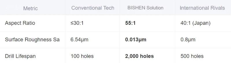
Tool Life Myth: A single PCD drill can continuously process 2,000 holes, which is 20 times longer than the imported tool life, and the cost is reduced to less than 5 yuan per hole;
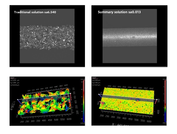
Nano-level surface revolution: The hole wall roughness Sa is reduced from 6.54μm to 0.013μm (a decrease of 99.8%), which is better than the aerospace optical mirror polishing standard (ISO 10110-8);
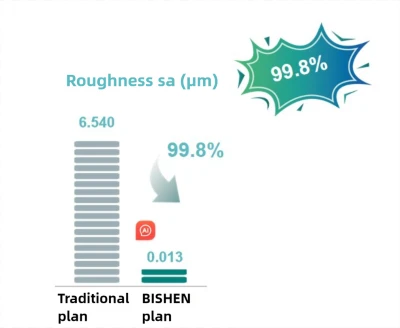
Zero defect processing: The edge collapse rate at the entrance is zero, and the roundness error is reduced to 0.003mm (equivalent to 1/3 of the diameter of human red blood cells);
Deep-to-diameter ratio limit: 55:1 processing capacity breaks the 2030 technology node predicted by the International Technology Roadmap for Semiconductors (ITRS) and reaches the standard 7 years ahead of schedule.
Technology Benchmarking (vs Global Competitors)
Processing comparison
Industrial Impact
From Single Case to Ecosystem Transformation
This breakthrough has catalyzed cross-industry innovations:
Semiconductor Localization:3D NAND via-hole processing efficiency surged 300%, reducing Yangtze Memory's production costs by 18%.
Photovoltaic Cost Revolution: Heterojunction solar cell back-electrode microhole yield jumped from 72% to 98%, cutting costs by ¥0.4/W per panel.
Space Optics Advancement: Enabled sub-10nm subsurface damage silicon microhole arrays for China's "Xuntian" space telescope, boosting imaging resolution by two orders of magnitude.
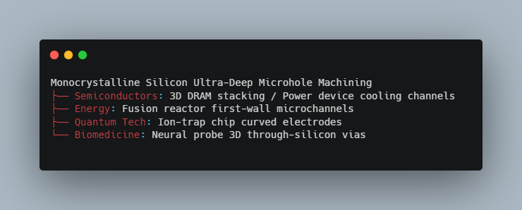
Technology Diffusion Map
MID profile:
MID pioneers precision metal manufacturing for small-batch, high-mix production, integrating CNC machining (±0.002mm), sheet metal fabrication, and industrial 3D printing. Specializing in semiconductor, medical, and new energy sectors, we deliver custom components with AI-driven quality control (defect rate <0.5%) and ultrasonic-assisted processes (Ra ≤0.4μm). Our agile production systems slash lead times by 40% while reducing costs 30-50%, empowering clients from prototyping to volume scaling with ISO-certified precision.


