



When it comes to manufacturing parts for semiconductor and photonics equipment, it's not just about microns-it's also about materials that push CNC machining to its physical limits. Components such as wafer chucks, plasma chambers, and alignment fixtures are increasingly made from ultra-hard materials like ceramics, tungsten carbide, or hardened stainless steels.
The Challenge: When the Material Fights Back
Ultra-hard materials are essential for durability, thermal stability, and corrosion resistance, especially in high-vacuum and high-temperature semiconductor environments. But they bring major challenges:
Extremely high cutting forces
Rapid tool wear, even with coated carbide or diamond tools
Microcracking or thermal deformation under conventional machining
Take advanced ceramic components, for instance. In one project involving a silicon nitride wafer support ring, the material's hardness exceeded HRA 90. Standard tooling failed in minutes, and heat buildup caused surface microfractures.
Why Conventional Machining Fails
Traditional machining setups struggle with these materials because:
Standard end mills cannot withstand the hardness
High friction leads to excessive heat, which distorts the part or reduces tool life
Vibration or chatter creates brittle fractures in ceramics or carbides
This makes it especially difficult to maintain tolerances in parts with tight dimensional constraints, such as optical lens holders or metrology frames.
Our Approach: Toolpath Strategy + Process Engineering
At MID Precision, we don't treat these parts like standard jobs. We:
Use PCD, CBN, and diamond-coated tooling designed for ultra-hard substrates
Apply low-force, high-speed cutting with optimized feed rates and dwell times
Employ coolant isolation or dry machining when thermal sensitivity is critical
Incorporate in-process inspection to catch cracks or surface anomalies before final pass
Real-World Case: Machining High-Purity Ceramic Mounts
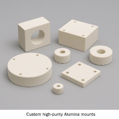
A global lithography OEM tasked us with machining custom high-purity alumina mounts with <±5 μm tolerance. Using a controlled micro-cutting strategy, specialized jigs, and multi-pass finishing, we completed the parts with zero microcracks and extended tool life by over 30%.
Built for Tough Materials, Trusted in High-Tech
Whether it's machining zirconia parts for ion implantation or tungsten alloy fixtures for X-ray imaging systems, we bring the expertise, tooling, and process control needed to tackle what others avoid.


