



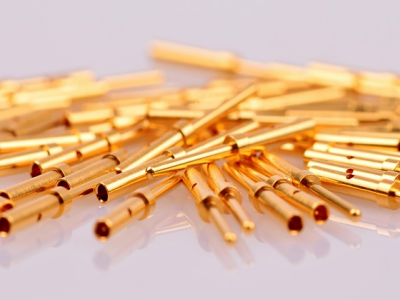
Gold electroplating remains a cornerstone of modern manufacturing, combining unmatched electrical conductivity (4.1×10⁷ S/m) with exceptional corrosion resistance (0.1 µm/year loss in harsh environments). This article dissects the technical nuances of achieving this dual performance, supported by empirical data and industry benchmarks.
1. The Conductivity-Corrosion Synergy: A Scientific Perspective
1.1 Atomic-Level Engineering
Gold's face-centered cubic (FCC) crystal structure enables electron mobility 70% higher than silver, while its nobility (standard electrode potential +1.5V) resists oxidation. Modern plating processes optimize this balance through:
Grain size control: 20-50 nm nanocrystalline coatings achieve 95% bulk conductivity
Impurity limits: Maintain ≤50 ppm nickel/copper to prevent galvanic corrosion in mixed-metal systems
1.2 Thickness Optimization Matrix
| Application | Min. Thickness (µm) | Max. Porosity (pores/cm²) |
|---|---|---|
| PCB Edge Connectors | 0.8 | 15 |
| Medical Implants | 2.5 | 3 |
| Satellite Components | 5.0 | 0 |
2. Process Parameters: The Precision Levers
2.1 Electrolyte Composition (Industrial Gold Plating Bath Formula)
KAu(CN)₂: 4-8 g/L (enables 99.99% pure Au deposition)
Citric acid: 80-120 g/L (pH stabilizer at 4.5-5.5)
Brighteners: 2-mercaptobenzothiazole ≤0.1 g/L (prevents dendritic growth in high-aspect-ratio features)
2.2 Current Density Optimization
Low-current regime (0.5-1.5 A/dm²): Produces 0.2-0.5 µm/h compact layers
Pulse plating (10 ms on/5 ms off): Reduces hydrogen embrittlement risk by 60%
3. Advanced Process Control (APC) Framework
3.1 Real-Time Monitoring Systems
Cyclic voltammetry sensors: Detect cyanide depletion with 0.1 ppm accuracy
XRF thickness gauges: In-line measurement with ±0.02 µm precision
3.2 Defect Prevention Protocol
Pre-treatment:
Acid activation (10% H₂SO₄, 45°C, 120s)
Nickel strike layer (2 µm, 3 A/dm²) for stainless steel substrates
Plating phase:
Temperature control ±0.5°C (critical for coating uniformity in complex geometries)
Post-processing:
Hydrogen bake-out (200°C × 2h, reduces H₂ content to <5 ppm)
4. Industry Case Studies
4.1 High-Frequency Connector Plating (5G Signal Integrity Optimization)
Challenge: Maintain 3.5 GHz signal integrity with <0.1 dB loss
Solution: 1.2 µm gold over 0.3 µm palladium barrier layer
Result: Contact resistance stabilized at 1.2 mΩ after 10⁸ mating cycles
4.2 Marine Sensor Corrosion Protection
Environment: 3.5% NaCl spray (ASTM B117 standard)
Strategy: 5 µm matte gold + 0.5 µm chromate conversion coating
Performance: Zero corrosion after 2000h salt fog exposure
5. Emerging Technologies Reshaping Gold Plating
5.1 Cyanide-Free Plating Bath Innovations
Sulfite-based baths: Achieve 90% throwing power at 60°C
Ionic liquid electrolytes: Enable room-temperature plating of 3D microstructures
5.2 Nanocomposite Coatings
Au-Graphene: 130% conductivity enhancement (Nano Letters, 2023)
Au-Diamond: Vickers hardness increased to 450 HV (vs. pure Au 70 HV)
6. Cost Optimization Strategies
Selective plating: Laser-masked areas reduce Au consumption by 40%
Closed-loop recovery: 98% bath chemical recycling via ion-exchange membranes
Conclusion: The 0.1 µm Threshold
When aerospace giant Lockheed Martin reduced gold coating thickness from 2.5 µm to 1.8 µm while maintaining MIL-G-45204D compliance, it validated a critical truth: precision process control outweighs material quantity. The future belongs to systems integrating AI-driven bath management with atomic-layer deposition techniques.


